PRODUCTS
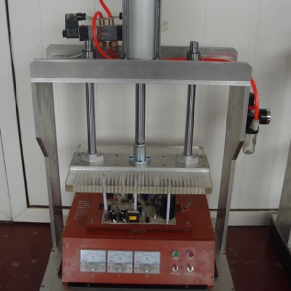
- Pneumatic Test Fixture
- Manual Test Fixture
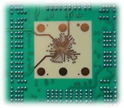
- Probe Cards
- RF Probe Cards
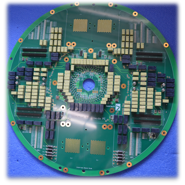
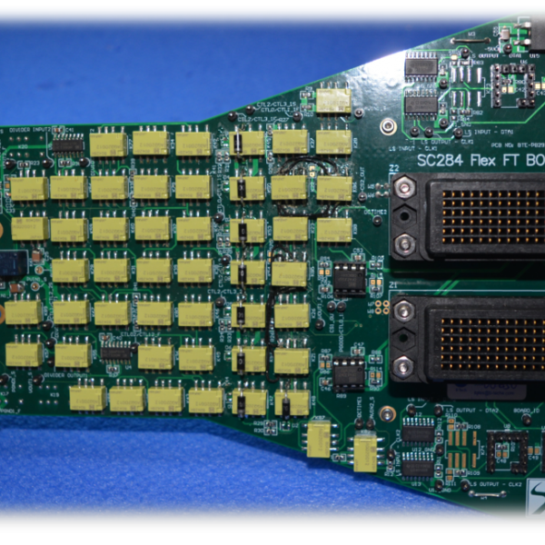
- Final Test Boards
- RF Final Test Boards
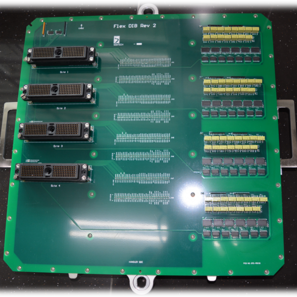
- Tester Interface Boards
- Burn-In Mother Boards
- Burn-In Rider Cards
- Evaluation Boards
- Electronic Control Boards / Modules
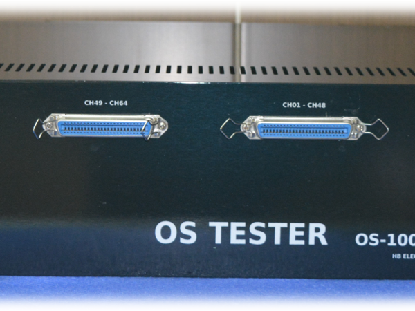
- Open Short Tester
- Wireless Shooting Target System
1
Conceptual Discussion/ Design
2
Schematic
3
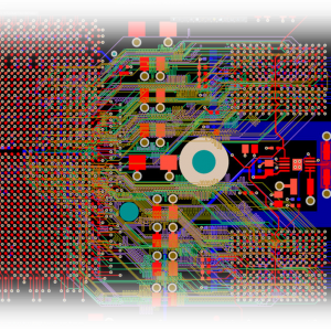
Layout
4
Board Fabrication
5
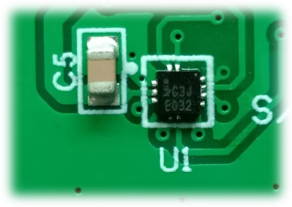
Assembly
6
Inspection
SOFTWARE
Altium Designer
- Schematic creation/editing
- PCB layout
- Design error check
- Gerber exporting/reviewing
Graphic Code
- Gerber importing/exporting
- Accessing GWK file
PCB FABRICATION CAPABILITY
| DESCRIPTION | CAPABILITY |
| Max Layer | 32 |
| Max Board Size | 686mm x 508mm |
| Max Board Thickness | 6mm |
| Min Board Thickness | 0.4mm (4 layer) |
| Board Thickness Tolerance | |
|---|---|
| t < 1.0mm | +/-12% |
| t >= 1.0mm | +/-10% |
| Material |
|
| Inner Copper Thickness | 1/3oz, 1/2oz, 1oz, 2oz |
| Outer Base Copper Thickness | 1/3oz, 1/2oz, 1oz, 2oz, 3oz |
| Min Trace Width | 2.4 mil |
| Min Copper Clearance | 2.4 mil |
| Min Hole Diameter | 0.1mm |
| Electrical Test | Flying probe |
| Leadtime | |
| 2 Layers | 5 to 7 working days |
| 4 to 12 Layers | 10 working days |
| 14 to 24 Layers | 10 to 22 working days |
| above 24 layers | 25 to 28 working days |
1
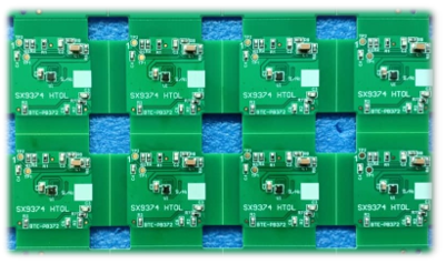
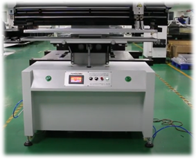
Solder Paste Printing
2
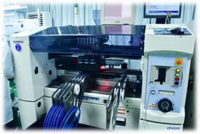
Component Mounting
3
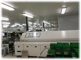
Reflow Soldering
4
Ultrasound cleaning
(if required)
5
De-panelise
6
Inspection
ASSEMBLY CAPABILITY
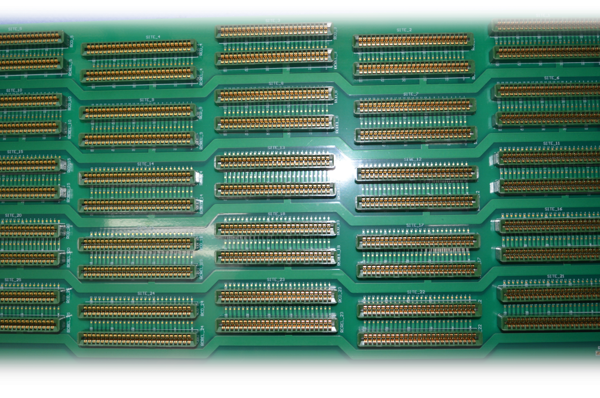
| ASSEMBLY TYPE | Surface Mount (SMT),Thru-hole, Mixed Technology (SMT/Thru-hole).Single and double sided SMT/PTH, Large parts on both sides, BGA on both sides. |
| STENCILS | Laser cut stainless steel |
| COMPONENTS | Passive components smallest size 0201, Fine pitch components smallest size 0.3mm pitch, BGA& DFN, Connectors and terminals |
| COMPONENT PACKAGING | Reels, Cut tape, Tube and Loose part |
| INSPECTION | Flying Probe for bare PCB, Visual and Microscope to 20x, Functional test upon request </td |
| SOLDER TYPE | Lead-free/ROHS compliant |
| SURFACE MOUNT CONNECTORS | Yes |
| PCB FINISH | Lead-free HASL, Electrolytic gold, Immersion gold |
| PANELIZED PCB | Tab routed, Breakaways tabs, V-Scored and Routed+ V scored |
| DESIGN FILE FORMAT | Garber RS-274X,274D, Altium Designer Source file, GC Prevue GWK-file |
| LEADTIME | 1 – 5 Days, 1-2 Weeks and Scheduled Deliveries |
| PARTS PROCUREMENT | Full Turnkey, Partial Turnkey and kitted/consigned |

